Bare Metal STM32

Periodically I have to bring up a new device and my current favorite processor line is the STM32 Cortex ARM processors from STMicroelectronics.  When bringing up new hardware, JTAG debugging (or similar) is immensely useful and ST provides tools to make that easy including:

    • ST-Link V2 hardware debug interface – you can buy an official ST-Link V2 for $23 from Digikey or elsewhere or purchase a nicer clone on eBay for $3.25.  ST evaluation boards such as for the STM32L476 Discovery or STM32F4 Nucleo (with mBed support too!) cost $10-20 and include an ST-Link on board that you can disconnect from the evaluation processor and connect to your target via the SWD connector and by removing the two ST-LINK jumpers.  You’ll need to connect the SWD connector to Vcc, Gnd, SWCLK, SWDIO, and NRST on the target.
    • Use the GCC ARM Embedded development tools to build your software.  Build an .elf with debug information and a .hex file for programming.
      • For Ubuntu platforms see here for installation via package manager.
    • Use the ST-Link utility to flash your .hex file to the target using the ST-Link V2
    • Use Texane STLink to make your target debuggable via the ST-Link V2 and GDB (see this post for details on linux setup for texane)
    • Debug, by running the texane STLink utility and you should see something like this:

STLINK GDB Server v0.5.6 (Mar 24 2013 10:29:19)
Many thanks to the STLINK development team.
(https://github.com/texane/stlink)

2016-02-29T16:18:14 INFO src/stlink-common.c: Loading device parameters….
2016-02-29T16:18:14 WARN src/stlink-common.c: unknown chip id! 0x10036415
Chip ID is 00000415, Core ID is  2ba01477.
KARL – should read back as 0x03, not 60 02 00 00
Listening at *:4242…


  • Launch gdb for your executable, connect to the target, and start debugging:

arm-none-eabi-gdb myProgram.elf
(gdb) target remote localhost:4242
(gdb) break main
(gdb) continue


  • GDB has a huge set of commands; see the manual here .  For example:
    • step  (or ‘s’)                (step through one source line – steps into functions)
    • stepi (or ‘si’)                (step through one assembly instruction)
    • next (or ‘n’)                  (step over a function)
    • break *0x8004060       (set breakpoint at address)
    • break main                  (set breakpoint at function)
    • info breakpoints          (or info b)
    • del 3                            (delete breakpoint # 3)
    • info registers
    • info reg $r3
    • p <variable_name>   (print value of variable)
    • p/x  $r3                       (print value in register r3 in hex)
    • list                               (list source code)
    • disassemble              (disassemble around current PC)
    • display $pc                 (show value in program counter with each step)
    • display/i $pc               (disassemble code at program counter with each step)
    • display/20i $pc           (disassemble 20 lines starting at pc with each step)
    • x/20i *0x08004060      (disassemble 20 lines starting at address 0x8004060)
    • x/20xw $sp                 (dump 20 longwords from stack)
  • Note that a watchdog interrupt will appear as a SIGTRAP

ZTW 7×7 CNC machine

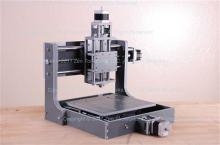
After reading a bunch of positive reviews, I purchased a Zen Toolworks 7×7 CNC machine on eBay.  It came with three SST43D2121 stepper motors, a 3-axis Univelop TB6560v2 motor controller , and a spindle (high speed 36v milling motor).  There is a remarkable absence of documentation for this stuff on the internet…hopefully this blog post will help.

I purchased a a MeanWell model S-100F-12 12v power supply ($20 on eBay) that supplies 12V/8.5A and connected it to the +7, +12v, GND inputs on the motor controller; numerous posts indicated that the 7v input can take 12v and so far I’ve had no problems with that.

ztw7x7

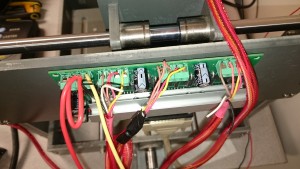
The wiring to the stepper motors is just as described on ZTW’s website:

2015-07-17 19.51.04

Stepper motor wiring

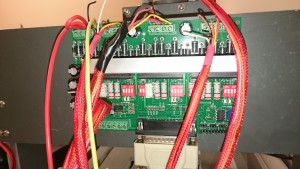
The motor controller has two sets of DIP switches for each motor: one has 2 switches and the other has 4 switches.  On the 2x switches I set 1,2=ON.  On the 4x switches I set 1=ON and 2,3,4=OFF.

DIP Switches

DIP Switches

This configures the motors for minimum (20%) current and smoothest movement (1/16 microsteps, 0% decay).  This was determined by trial and error.  Using the lowest load setting was important because the software I’m using (LinuxCNC) turns the motors on when powered; they are either held locked in place or driven (moving) but never turned off; so they are constantly drawing power…with 20% current, they stay cool and the 12v supply is never drawing more than 9.x Watts for all 3 motors and the controller.  Using the 1/16 microsteps made a huge difference in smoothness of movement; otherwise moving the motors was very noisy.

The motor controller connects to the computer using a straight-through DB-25 cable.  The pins are used as follows:

2 = Out = Step X
3 = Out = Dir X
4 = Out = Step Y
5 = Out = Dir Y
6 = Out = Step Z
7 = Out = Dir Z
8 = Out = Enable Y
9 = Out = Enable Z
14 = Out = Enable X
10 = In = Emergency Stop (low***)
11 = In = Limit X (low***)
12 = In = Limit Y (low***)
13 = In = Limit Z (low***)
1,15,16,17 = N/A = Not Utilized
18-25 = GND
***Signals are Active Low

Note that the Enable line must be active (high) for a motor to turn.  When properly configured, the software will enable the motor when the machine is powered and disable the motor when the emergency stop button is pressed (in software or hardware) which powers-down the motors.

I’m using LinuxCNC for the control software; it’s free and I like linux.  You can read about it here.  The software is extremely configurable which makes figuring the setup out problematic.  The software comes with two configuration wizards; one is for stepper-motor-based machines.  I used this and created a configuration file named ztw7x7, but the wizard doesn’t allow you to configure the Enable pins properly.  In the end, I had to edit the .hal file by hand to add definitions for Xenable, Yenable, and Zenable.  This link was very helpful.  I’ll post the edited file shortly.

There are many good choices for controlling NEMA17 stepper motors (1.2A/phase) including Arduino (Uno or Mega2560) with GRBL software (optimized for Mega2560 here) with a CNC shield using the Allegro A4988 or  TI DRV8255 drivers (1-2A w/fan) or TB6600 stepper motor drivers (3.5A).  See install info here.  Note that the drivers must be adjusted for max current and many suggest adding over-voltage protection for them including a 100uF cap across the motor. I would consider a suitably sized TVS diode instead because most 100uF caps aren’t rated for the ripple current they would experience.

Replacement spindles are available with 775 motors and the same ER11 spindle.

DIY PCB single-sided success

I am finally having success making single-sided PCBs at home using the toner transfer process.  I am generally using traces no thinner than 12 mils (although I think I did 10 mils a few times and it worked fine) and 12-15 mil spacing. With modern surface-mount parts, it’s amazing how much of the circuit can be done in a single layer and without drilling.

I’m using products from PulsarFx that are specifically made for this process and they work much better.  I came tantalizingly close many times using McGyver methods (magazine paper, clothes iron, etc.), but it never worked quite right and cost many hours of frustration.  In particular, getting the paper to release from the toner was always a problem and I often experienced over-etching.  I tried magazine, matte, and many varieties of glossy paper from Staples.  In the end, the PulsarFx products are not that expensive and work perfectly.

I have no relationship with PulsarFx other than that I am a customer and am now a fan.

The current process:

  • Print on PulsarFx toner transfer paper using an HP 1025nw printer.  Printing did not work well with my Canon D420 printer (did not put enough toner down) and I couldn’t feed the thick transfer paper through my Samsung ML-1865W or ML-2160.  The transfer paper is coated with a material that dissolves quickly in water, so after the toner is transferred to the copper board, the paper releases perfectly every time.  Configure your printer for thick glossy paper, black or grayscale, and maximum toner output.
  • Clean a blank copper board to a bright shine using steel wool.  I get the blank copper-clad boards on eBay from seller abcfab; ideally you should use 1/2oz copper for much faster etching, but I’ve also had success etching 1oz and 2oz copper.  After cleaning with steel wool, I’ve tried using tarn-x and/or acetone and they may help slightly but I’ve had good results without them.  Once the board is bright and shiny everywhere, don’t touch it with your bare hands…use gloves to avoid getting skin oil on it.  I use nitrile disposable gloves throughout this process; they cost $8 for 100 at Harbor Freight Tools.
  • Place the printed pattern face down (toner touching the shiny copper) on the copper board and run it several times (like 10) through a laminator.  I am using the PulsarFx “Applicator” which is just a big laminator.  I also have a much cheaper Harbor Freight Tools laminator which I am going to try and report on.  The board gets hot after a few passes through the laminator so I use leather work gloves.
  • After lamination, soak the board with the transfer paper stuck to it in water, I use a plastic tupperware container.  After a minute or two (sometimes within seconds), the paper’s coating dissolves and the paper just floats away from the copper board leaving the toner pattern on the copper.  Throw away the paper and pat the board dry with a paper towel. The water and container gets used again later in this process so keep it handy.
  • Follow the directions on the package and cut a sheet of PulsarFx Green Toner Reactive Foil a little larger than the copper board (2″ longer).  Place the foil dull-side down on the board and wrap 2″ under the board.  Place the side with the board with the 2″ wrapped under it in the laminator and try to keep apply some drag to the foil with your fingers as it goes through the laminator to prevent the foil from wrinkling.  I don’t have this quite right yet, but it still works pretty well.  I put it through the laminator a second time to make sure it has stuck.  Then peel the foil back from the board at a 180-degree angle.  What’s left is green foil covering most if not all of the toner.  The foil creates a stronger barrier to the etchant; without it, the etchant sometimes eats through the toner in places before the etching is finished resulting in pitting or uneven edges.  With the foil, I get perfect etching and nice clean edges, even with 2oz copper on the boards.
  • In another plastic (e.g. tupperware) container, mix the etching solution using nitrile gloves and chemical protective glasses, and preferably wearing old clothes: pour 1 cup of hydogen peroxide (purchased at my local supermarket) into the tupperware then mix in 1 cup of muriatic acid (hydrochloric acid) which I get in 1 gallon containers from Lowes which costs around $5/gallon.  I use a disposable styrofoam coffee cup as a measuring cup.  Because this is a sadly litigious world: these are harsh chemicals; don’t get them on your skin, on your clothes, or in your eyes; it is acid, it’s dangerous.  Use proper protective gear, if you don’t know how to handle chemicals, don’t do this.  Proceed at your own risk.  I do this in the back yard because the fumes (and liquid) can be corrosive to nearby metals.  I am going to try this again with the white vinegar/peroxide/salt etching method and report back.
  • Place the copper board in the etching solution with the pattern facing up; every minute or two gently brush the surface of the board with a foam paint brush (around $0.79 from Lowes).  Brush it a few times to brush away the etched material and expose more shiny copper; this makes the etching process go much faster.
  • When the copper is all gone and only the toner/transfer foil is showing, remove the board from the etchant and place it in the other tupperware container containing just water to stop the etching.  Note: the etchant solution doesn’t seem to effect the nitrile gloves so I just take it out by hand.
  • Carefully (gloves, chemical glasses) pour the etchant into a plastic container for storage and/or disposal.  I use a plastic funnel and a plastic bottle that seals liquid tight (e.g. an iced tea or juice bottle).  Take your time doing this so nothing splashes out.  Seal the bottle, then rinse clean your brush, tupperware, circuit board, etc.  You can’t just pour the used etchant down the drain (it is toxic and will probably ruin your pipes).  Take it to your local recycling/waste disposal facility for proper disposal (I’m looking into ways to manage this better).
  • The final step (for me, for now) is to remove the toner and foil from the board.  This is done using a rag or paper towel and acetone (which also costs around $5/gallon at Lowes).  Do this outside too, acetone is very smelly.

When you are done, you will have a nice shiny PCB ready to solder (or drill if you are still using through-hole parts).  Total time is under 30 minutes.

  • For drilling, I use an old Dremel model 380 rotary tool and an old Dremel model 210 drill press (purchased on eBay for ~$20 shipped – they are commonly available there – note, this press only fits tool models 245, 250, 260, 270, 280, 350, 370, and 380). I’ve read that the 210 press is much more precise than the newer ones but I can’t confirm that.  I can confirm that this combination drills precise holes in the PCB.  I get carbide drill bits that fit the rotary tool from Harbor Freight Tools.  You can also get them from All Electronics or Ebay.

My next steps are to experiment with soldermask, silkscreen, photo-transfer, and multiple layers.  I’m also going to look into more environmentally friendly etchants or good ways to make the left over etchant non-toxic.

No more HP printers for me…

I’ve been grappling with HP’s CP1025nw printer for over a year and have concluded that HP is no longer capable of making a decent printer. This is sad because HP used to be the premier printer company.  I’ve been buying HP lasers for a very long time; I had an HP Laserjet Plus back in the 1980s when they cost a fortune, but after several dismal HP printers over the last 5 years, I will no longer purchase from them.

I bought this particular color laser printer mainly for its “network” feature. Unfortunately, it seems to disconnect from the network whenever it goes into power save mode and requires manual power cycling to re-connect. When disconnected it cannot be awakened or accessed by ping, http, or any other protocol. I have tried wired and wireless connections, static and dynamic IPs…no luck.  Many others have reported the same problem on multiple HP printer models.

Aggravating this is HP’s “technical support” whose goal seems to be to dissuade you from calling by repeatedly engaging in massive time-wasting exercises designed to help you understand how thoroughly ignorant they are of IP networking basics.  This too is sad as it reflects a change in many technology companies: they no longer attempt to reduce support costs by improving documentation and product quality but instead focus on reducing support costs and quality by outsourcing to folks who have little connection to or interest in their company or products.

On the plus side, I’ve had great experiences with Canon laser printers for the last several years and their supplies are cheaper too!

DIY PCBs

Although I’m a big fan of PCB-Pool, I’m trying to learn to make simple printed circuit boards at home instead of having to send out (and wait days or weeks). I’m attempting the toner-transfer method now; I don’t have it quite right yet, but it seems doable…with the right process.  It sounds great in concept:

  • Print the a mirror image of the pattern to be etched using a laser printer on suitable paper
  • Transfer the toner image from the paper to a blank copper clad PCB using heat and pressure (iron-on)
  • Etch the PCB with the toner acting as resist
  • Use acetone to remove the toner leaving the desired copper pattern
  • Optionally tin plate
  • Drill and mount components!

So far, my main obstacle has been clean and heavy toner transfer. I’ve been able to transfer some fairly fine patterns (15 mil lines with 15 mil spacing), but invariably some of the toner doesn’t transfer and then touch-ups are required. Also, the toner appears to have some holes in it which results in pitting during etching. Using sharpie to touch up the toner seems to help a bit, but the sharpie often is removed in the etching process.

  • Pages from a regular magazine (e.g. IEEE spectrum) that are thin and glossy seem to work better than expensive thick glossy paper. The toner transfers onto the page and the page releases it onto the circuit board fairly cleanly. The ink on the magazine page seems irrelevant to the process.
  • Blank copper clad boards are cheap and plentiful on eBay.
  • Preparing the blank board with a scrunge and tarn-x seems to help.
  • I’m using a harbor-freight $30 laminator to do the toner transfer…I can’t yet tell if it works better than an iron…I need to do some head-to-head experiments.  The PCB + paper just barely fits through the laminator and requires a bit of a push to get started.  I make 6 or 7 passes through the laminator then soak the board in water to get the paper off.
  • 2oz copper cladding takes a long time to etch…need to get some 1/2oz
  • No success with sponge-etching…it mainly removed toner.
  • Peroxide/vinegar/salt etchant seems to work, but slowly…I need to work more with this. It is certainly a much safer chemical process.
  • Even the old standby ferric chloride seems to take a long time…I may need to get/build a more sophisticated etching tank (heater+agitator or sprayer)…and then there’s the disposal problem.  I was mixing my own and may not have made it strong enough
  • HCl (Muriatic acid) + H2O2 etching seems to work very fast, but it is quite aggressive and eats away a lot of the resist.

If I can’t get this to work reliably, I’m going to try a commercial toner transfer solution and then try using photoresist which may cost a bit more, but might save lots of time and aggravation.  I also ordered a CNC machine which will, I hope, automate the drilling of vias and through-hole pads. (and can also be used for isolation routing of boards to eliminate etching entirely in some cases).

More ChibiOS

I’m really enjoying ChibiOS.  The hardware abstraction layer is beautiful and the OS is rich, fast, and compact.  I am using it for a wireless IP gateway application.  I’m doing some pretty low-level stuff (interrupt driven SPI communications with a transceiver) and I have not had to write any processor-specific code!  I’m still getting to know ChibiOS, but I already have an application running on development boards that is communicating via the wireless transceiver, pulling an IP address via DHCP, serving a web page and a command shell via TCP, and also a separate serial command shell.  It fits in 80K.  By the end of next week, I hope to have a first cut of fully operational application software and move on to the custom hardware design.

Chibi/OS

Using NetBeans and Gnu ARM tools, I was able to build and run the ChibiOS/RT demos for the STM32F4 discovery board.  I downloaded the zip file containing the latest version of ChibiOS/RT and extracted it to my NetBeansProjects folder.  To build a project:

  • File -> New Project -> C/C++ -> C/C++ Project with Existing Sources
  • Browse to the appropriate directory e.g:
    • …./NetBeansProjects/ChibiOS_2.6.7/demos/ARMCM4-STM32F407-DISCOVERY
  • Select Tool Collection as GNU ARM
  • Select Automatic Configuration Mode

That’s it, the project is imported and automatically builds!  You can load it onto the target using st-flash and debug it (if desired) using st-util:

  • st-flash write \Users\dalbert\Documents\NetBeansProjects\ChibiOS_2.6.7\demos\ARMCM4-STM32F407-DISCOVERY\build\ch.bin 0x8000000
  • st-util  (make sure you’ve configured build/ch.elf as the project Properties->Build->Make->Build Result)

I’ve built and tested the three STM32F4-DISCOVERY demos and they all ran successfully including the VCP USB comm port with command interpreter in the MEMS demo.

I’ve also built the ChibiOS/RT + lwIP + PPP application here which required a few fixes and must be linked with ChibiOS/RT 3.x but then runs nicely using the serial port (PA2, PA3) to serve a PPP connection.  I have two directories under NetBeansProjects:
stm32f4-chibios-lwip-pppos-master
ChibiOS_3.0.x
Then I create a symlink under stm32f4-chibi-…-master/lib called ChibiOS-RT that links to ../../ChibiOS_3.0.x.

On the remote terminal (linux box) side, I configured /etc/ppp/options including the serial port I was connected to (/dev/ttyUSB0) and the baudrate (38400); the whole file looks like this:

# Prevent pppd from forking into the background
-detach
debug
/dev/ttyUSB0
38400
# wait for connection if none initially found
passive
# no hardware flow control
nocrtscts
# don’t use modem control lines
local
# create a default route for this connection in the routing table
defaultroute
# no authorization required
noauth
# ensure exclusive access to the serial device
lock
# do not set up any escaped control sequences
asyncmap 0
# use a maximum transmission packet size of 552 bytes
mtu 552
# use a maximum receive packet size of 552 bytes
mru 552
# IP stack configuration
netmask 255.255.255.0
noipdefault
:

Launch pppd specifying localip:remoteip: which generate the ppp0 network interface (shows on ifconfig):

sudo pppd 172.30.1.98:172.30.1.99

Reset the discovery board and the PPP connection is up!  You can ping the discovery board (ping 172.30.1.99) and can bring up a remote shell connection using netcat: nc 172.30.1.99 25  (note to send a CR requires Ctrl-V <enter><enter>).


Cortex Cross Development Environment

I’ve been using ARM processors with C/C++ for more than a decade for nearly all of my embedded development.  I’ve usually used Em::Blocks on Windows platforms which works nicely but doesn’t fully work on linux, doesn’t support integrated version control, and hides some details that I want to have control over.

I’m working on some new projects using Cortex M3 and M4 processors and wanted to explore the available tools.  My favorite IDE is still NetBeans.  Netbeans was meant for Java, but has a C/C++ plugin and is fairly easy to configure for gcc cross-compilation using gnu tools for arm (linux/mac/windows).  I’d really like to get the environment working both on windows and linux since I routinely use both.  This post details the linux setup:

1) Download and install the GNU tools for ARM in /usr/local/gcc-arm-none-eabi-…:

cd /usr/local
sudo tar xjf ~dalbert/Downloads/gcc-arm-none-eabi-*.bz2

Add the tools to the search path (add the following to ~/.bashrc):

PATH=$PATH:/usr/local/gcc-arm-none-eabi-4_9-2014q4/bin

2) Install the C++ plugin for Netbeans and configure NetBeans to use add the new arm cross-compilation toolchain:

Tools->Options->C/C++->Add the configure the base directory (e.g. /usr/local/gcc-arm-none-eabi-4_9-2014q4/bin) and the c, c++, assembler, and debugger programs to arm-none-eabi-gcc, arm-none-eabi-g++, arm-none-eabi-as, arm-none-eabi-gdb.  I add the cross tools as GNU_ARM

3) Install the GDB Server plugin for Netbeans.  This allows you to attach NetBeans debugger to the remote target using the configured gdb debugger (arm-none-eabi-gdb per the above step).  To debug, Debug->Attach Debugger, choose debugger type as “gdbserver”, choose target as “remote:4242”, and set the project to your project.

4) For hardware assisted debugging, the STMlinkv2 software works with the STLink USB JTAG/SWD debug hardware ($30 from Digikey and included free with any ST Discovery board; I like this one that costs $10 at Digikey); documentation is here.

Install texane stmlinkv2 (for linux, install the packages required to build stmlinkv2: autotools autoconf autogen libusb-1.0.0 and maybe libusb-1.0.0-dev, intltool) see here and here for more info.  Windows binaries are here.  Included is st-flash for flashing the processors, st-info, st-term, and st-util: a GDB server.  For Windows, just unzip the folder to a convenient location and run st-util.  For linux, after installing the dependencies (listed above), build STMLinkV2 and install it (installs in /usr/local/bin):

./autogen.sh
./configure
make
sudo make install

Grant permissions for the tools (e.g. st-util) to access the USB ST-Link V2 hardware:

sudo install -m 644 49-stlinkv2.rules /etc/udev/rules.d/49-stlinkv2.rules
sudo udevadm control –reload-rules

More info on permissions for st-util

5) Download sample code and create a project for one of the examples.  I keep my NetBeans projects in my home directory in a NetBeansProjects directory:

File->New Project->C/C++ Project with Existing Sources->~/NetBeansProjects/kkstm32_base-master/example/32l_lcd
Set the Tool Collection to GNU_ARM and select Automatic configuration mode then press finish.
Note: the STM32 library in the downloaded example code I’ve linked to contains an error in core_cm3.c that must be fixed (add the ‘&’ in front of result r); see diffs below:

dalbert@mypc ~/NetBeansProjects/kkstm32_base-master/libs_stm/inc/core_support $ diff core_cm3.c.orig core_cm3.c
736c736
<    __ASM volatile (“strexb %0, %2, [%1]” : “=r” (result) : “r” (addr), “r” (value) );

>    __ASM volatile (“strexb %0, %2, [%1]” : “=&r” (result) : “r” (addr), “r” (value) );
753c753
<    __ASM volatile (“strexh %0, %2, [%1]” : “=r” (result) : “r” (addr), “r” (value) );

>    __ASM volatile (“strexh %0, %2, [%1]” : “=&r” (result) : “r” (addr), “r” (value) );

cd kkstm32_base-master/libs_stm/build
make     (to build the STM32 peripheral library)
cd kkstm32_base-master/example/32l_lcd
make     (to build the example code – builds lcd.elf, lcd.bin)

6) Build and load one of the examples built above into your STM32L Discovery eval board using the CLI first to confirm that everything is working:

st-flash write lcd.bin 0x8000000
test the other nifty st tools: st-info, st-term, st-util

7) Test debug interface from CLI:

st-util   (runs gdb-server which listens on localhost:4242)
arm-none-eabi-gdb -q lcd.elf
(gdb) target remote localhost:4242

8) Optionally install openocd (gdb server compatible) and test it for debugging:

sudo apt-get install openocd       (installs to /usr/share/openocd)
openocd –version
sudo openocd -f /usr/share/openocd/scripts/interface/stlink-v2.cfg -f /usr/share/openocd/scripts/target/stm32lx_stlink.cfg
in another window: telnet localhost 4444

9) Import one of the example projects into NetBeans and test operation in the IDE!

File->New Project->C/C++->C/C++ Project with Existing Sources
Choose source folder and GNU_ARM tool collection
Select Automatic Configuration Mode
Right click the project->Properties->Build->Make->Build Result = build/ch.elf

Make sure the Makefile is compiling the project with debugging enabled (-g)

Other links related to setting up a gnu/arm cross development environment:

  • https://github.com/texane/stlink/wiki   (wiki for the stlink tools)
  • http://gpio.kaltpost.de/?page_id=148  (detailed discussion of stlink tools)
  • http://embeddedprogrammer.blogspot.co.uk/2012/09/stm32f4discovery-development-with-gcc.html  (very detailed article on eclipse, openocd, and a wide range of cross tools)
  • http://hertaville.com/2013/09/02/stm32f0discovery-part-1-linux/
  • http://gnuarmeclipse.livius.net/blog/test-project/
  • LibOpenCM3
  • http://www.ba0sh1.com/opensource-stm32-development/
  • http://false.ekta.is/2012/05/using-netbeans-for-stm32-development-with-stlink-texane/
  • http://www.emb4fun.de/arm/lwipuhttp/
  • https://bitbucket.org/philpem/stm32_spl   (STM32 peripheral library)

Next steps:

Solar Power

I’m considering adding solar power to my house.  I’m not interested in leasing.  The cost of solar power continues to plummet and now soft costs (non-hardware) are about half of the total cost.  The national average cost installed before incentives is now around $3.6/Watt and Maryland costs are around the national average.  Interestingly, America is still the most expensive country in which to install photovoltaics; in Germany it is *much* less expensive…the free market doesn’t seem to be working so well in that regard (much like our health care or telecommunications systems).

Although the green aspects of solar power appeal to me, it needs to make financial sense too.  In 2014 I paid $2130 for delivery of an average of 1328kWh/month = $178/month ~= $0.134/kWh.   electricity.  Given Maryland’s daily hours of insolation (around 4.2), to offset my usage I’d need a 15kW system which would cost around $54K before incentives/rebates/etc.

I met with a reputable local solar installer and received a quote; they performed a detailed analysis of my house roof and estimated that my maximum array size would be 46 panels x 270W/panel = 12.42kW.  Given the panels’ locations, angles, etc. they estimated that they would generate 1093 kWh/kW/year or 13,570kWh/yr.  They did not use any sales pressure tactics and were very professional.  They used some higher end equipment and their terms are outstanding; the total cost was estimated at $48,680 (before credits) or $3.92/installed Watt which is somewhat higher than average ($3.6) but not unreasonably so given their warranty/support.

There is currently a federal 30% rebate and a $1K Maryland tax credit on the purchase of panels which brought the installed price to $33,426 ($2.69/installed Watt).  Maryland further adds Solar Renewable Energy Credits or SRECs for the energy you actually generate which traded at an average of $0.14/kWh in 2014.  This would yield an additional $1900/yr, but there’s no telling how long that will last.

The panels are permanent…the cost to remove and re-install would be prohibitive so they effectively become a part of the house.  Moreover, the cost of solar (and therefore the value of the panels) will continue to decline; the SunShot initiative targets an installed cost of $1 per installed Watt by 2020 and panel and inverter technology will surely continue to improve and the panels themselves have a limited (20-30 year) life…usually 25 year guaranteed.  So you can assume the panels have no value at the end of their life.

In some ways, with SRECs, this looks pretty appealing: $4K/yr * 25 years = $100K which corresponds to a 4.5% rate of return on the original $33K investment.  Moreover, although it has declined recently, electricity inflation has averaged 2-3% for the last 20 years, so the rate of return is really more like 6.5% to 7%.

The remaining question for me is how the scenario plays out if you sell your house before the end of the panels’ life (i.e. if you sell after 10 years, what value do the panels retain since they will continue to generate money for at least another 15 years)?

Update: Although I was very impressed with the solar company: Astrum Solar (now Direct Energy Solar) I ultimately decided against it.  If I were very confident I’d be in this house 10 years from now, I would buy the panels and I’d buy them from Astrum – they were very professional.  However the numbers didn’t work for me.  My house is fairly energy efficient and we have gas heat and hot water so our electric bill is already pretty low.  As a result, the ROI was 10+ years and if we decided to move after the kids were in college (6 years!), we’d potentially take a big loss on the system.  A realtor friend told us that panels don’t really affect the house price one way or the other; i.e. the panels would convey for free to the next owner or we’d have to go through an expensive process to have them taken down, shipped, and re-installed on the next house.  It’s just too big a risk.

It really amazes me that so many people enter into very long-term solar leases given the onerous costs if the lease is broken.  Leasing effectively requires any future buyer to assume the lease which might seriously encumber a sale.